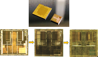
What is delayering in failure engineering, and why do you need to delayer parts?
Delayering is a process in failure engineering that involves selectively removing layers from a semiconductor device to expose the underlying components and conductors. This process is typically done using various chemical etching and mechanical polishing techniques to carefully remove layers one-by-one.
The need for delayering arises when the root cause of a device failure cannot be identified through non-destructive analysis techniques such as microscopy or X-ray analysis. By delayering the device, technicians can expose the internal components and conductors, allowing for more detailed and in-depth analysis of the device.
Delayering can also be used to analyze the quality of the layers themselves, as well as their thickness and uniformity, which can affect the device’s performance and reliability.
Delayering can be a complex and time-consuming process, requiring specialized equipment and expertise. However, it is an important tool in failure engineering, as it allows for more comprehensive and accurate analysis of the root cause of a device failure, and can help identify any underlying issues with the device’s design or manufacturing process.