Laser Decapsulation

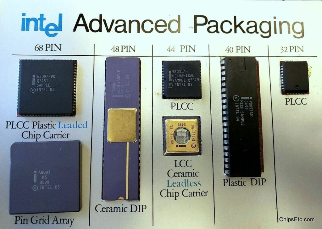
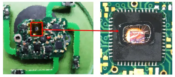
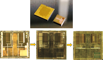
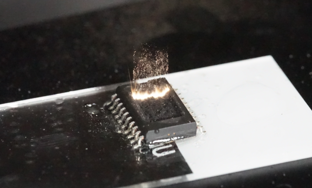
Laser-based decapsulation is an alternative method to traditional acid decapsulation for removing the protective cover from a chip package to expose the integrated circuit inside. This process uses a laser to ablate or vaporize the material covering the chip.

The laser used for decapsulation is typically a high-powered, pulsed laser, such as a Q-switched Nd:YAG or excimer laser. The laser energy is focused onto a small spot on the package surface, which causes localized heating and vaporization of the material. The laser beam is scanned over the surface of the package to remove the entire protective layer.

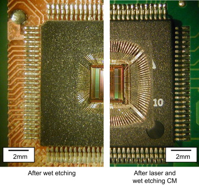
The advantage of laser-based decapsulation is that it is a non-contact and non-destructive method that can be used for a wide range of package materials, including ceramics and plastics. It also allows for precise control over the amount of material removed, which can be important for preserving the integrity of the integrated circuit inside.

Laser Decap

However, laser-based decapsulation also has some limitations. It can be slower than acid or dry/mechanical decapsulation for very dense packages, and the equipment required for laser-based decapsulation can be expensive. Additionally, laser-based decapsulation may not be suitable for certain types of package materials or structures.

For example, in a study published in the Journal of Microelectronics and Electronic Packaging, laser-based decapsulation of a plastic package with a protective layer thickness of 100 micrometers was completed in about 30 seconds using a Q-switched Nd:YAG laser with a pulse duration of 10 nanoseconds. In another study published in the Journal of Electronic Packaging, laser decapsulation of a ceramic package with a protective layer thickness of 180 micrometers was completed in about 2 minutes using an excimer laser.

However, the actual time required for laser decapsulation can vary depending on the specific laser used, the material of the package, and other factors. Additionally, the time required for laser decapsulation can be affected by the need to adjust laser parameters or the need to perform multiple passes over the same area to fully remove the protective layer.

In summary, laser-based decapsulation is a non-contact and non-destructive method for removing the protective cover from a chip package using a high-powered pulsed laser. While it has some advantages over traditional acid decapsulation, it also has some limitations and may not be suitable for all types of package materials or structures. As your decap partner and advisor, we will recommend the best decap type for your packages, cost, and size requirements.

Plastic vs Ceramic Decap

What’s the difference between plastic and ceramic chip packages?

Ceramic and plastic are two common materials used for chip packages in the electronics industry. Here are some of the main differences between them:

  1. Material: Ceramic packages are made of ceramic material, while plastic packages are made of plastic. Ceramic is more expensive than plastic, but it offers better thermal and electrical properties.
  2. Thermal properties: Ceramic has better thermal conductivity than plastic, which means it can dissipate heat more effectively. This makes ceramic packages more suitable for high-power applications where heat dissipation is critical.
  3. Electrical properties: Ceramic is also a better insulator than plastic, which makes it more suitable for high-frequency and high-voltage applications.
  4. Cost: Ceramic packages are more expensive than plastic packages due to the higher cost of the ceramic material and the manufacturing process.
  5. Size: Ceramic packages tend to be larger and heavier than plastic packages due to the need for a thicker material to provide adequate heat dissipation.

In summary, ceramic packages offer better thermal and electrical properties, but they are more expensive and larger than plastic packages. Plastic packages are less expensive and lighter, but they may not be suitable for high-power or high-frequency applications. Now that you know why your device may use different packaging materials, lets look at the implications for your decap process.

Example packaging types

What’s the difference in decapping a ceramic vs plastic chip package?

Decapping is the process of removing the protective cover from a chip package to expose the integrated circuit inside. The decapping process can be different for ceramic and plastic chip packages due to the differences in their materials and construction.

Ceramic chip packages are typically decapped using a mixture of nitric and sulfuric acid, which dissolves the ceramic material and exposes the integrated circuit. This process is called acid decapsulation. However, this process is very harsh and requires specialized equipment and expertise to carry out safely. Ceramic packages are also more durable and resistant to environmental factors such as heat and moisture.

On the other hand, plastic chip packages are typically decapped using a hot sulfuric acid or organic solvent, which dissolves the plastic material and exposes the integrated circuit. This process is less harsh than acid decapsulation, but it can still be dangerous if not done properly. Plastic packages are less durable than ceramic packages and may be more susceptible to damage from environmental factors.

In summary, the decapping process can differ between ceramic and plastic chip packages due to their material properties and construction. Ceramic packages require a more aggressive acid decapsulation process, while plastic packages can be decapped with a less harsh solvent. Additionally, ceramic packages are typically more durable and resistant to environmental factors than plastic packages. Here at DecapLab, we routinely decap both package types.

Decapsulation FAQ

  1. What is decapsulation in failure analysis? Decapsulation in failure analysis refers to the process of removing the encapsulation material or package from a semiconductor device to expose the underlying components for further analysis.
  2. Why do I need to decapsulate a device for failure analysis? Decapsulation is necessary when the root cause of a device failure cannot be identified through non-destructive analysis techniques such as microscopy or X-ray analysis. By decapsulating the device, technicians can expose the internal components and conductors, allowing for more detailed and in-depth analysis of the device.
  3. What are the different types of decapsulation methods? There are different types of decapsulation methods, including wet etching, laser/dry etching, and mechanical decapsulation.
  4. What is a flip-chip and can they be decapsulated? Flip chip decapsulation also requires a different technique for exposing the active surface of the chip once the protective layer is removed. Since the active surface of the chip is facing downwards in flip chip packaging, the chip must be flipped over after decapsulation to access the active surface.
  5. How do I choose the best decapsulation method for my device? The best decapsulation method for a device depends on factors such as the type of package, the encapsulation material, and the specific failure mode being investigated.
  6. What types of devices can be decapsulated? Most semiconductor devices can be decapsulated, including integrated circuits (ICs), microprocessors, and memory devices.
  7. What is backside preparation, and why is it important? Backside preparation is the process of thinning the substrate on the backside of the device to allow for better visualization of the internal components. It is important because it can significantly improve the accuracy and effectiveness of subsequent analysis techniques such as microscopy or X-ray analysis.
  8. Can I do decapsulation in-house, or should I outsource it to a service lab? Whether to do decapsulation in-house or outsource it to a service lab depends on factors such as the availability of specialized equipment and expertise, the complexity of the device, and the time and resources available for the analysis.
  9. How long does decapsulation typically take? The time required for decapsulation depends on factors such as the type of device, the encapsulation material, and the specific decapsulation method used. Typically, it can take anywhere from a few hours to several days.
  10. Is decapsulation a destructive process? Decapsulation is a destructive process, as it involves removing the encapsulation material or package from the device. However, it is often necessary to identify the root cause of a device failure.
  11. Are there any risks involved in decapsulation, such as damage to the device or exposure to hazardous chemicals? Risks associated with decapsulation can include damage to the device or exposure to hazardous chemicals. However, these risks can be minimized through proper equipment, training, and safety protocols.
  12. What kind of information can be obtained from decapsulation? Decapsulation can provide information such as the internal structure of the device, the quality of the encapsulation layers, and any signs of manufacturing defects or wear.
  13. How can decapsulation help me identify the root cause of failure in my device? Decapsulation can help identify the root cause of failure by exposing the internal components of the device and allowing for more detailed analysis of any defects or abnormalities.
  14. What are the limitations of decapsulation in failure analysis? Limitations of decapsulation include the potential for damage to the device during the process, the need for specialized equipment and expertise, and the potential for incomplete or inaccurate analysis if the device is not properly prepared or analyzed.
  15. How much does decapsulation cost? The cost of decapsulation can vary depending on factors such as the type of device, the encapsulation material, and the specific decapsulation method used.
  16. How can I ensure the confidentiality and security of my device and information during the decapsulation process? To ensure the confidentiality and security of the device and information during the decapsulation process, it is important to work with a reputable service lab that has appropriate security protocols and procedures in place. This can include measures such as restricted access, secure storage, and non-disclosure agreements.

Wet vs Dry Decapsulation

What is the difference between wet and dry decapsulation?

The main difference between wet and dry decapsulation is the method used to remove the outer layers of the microelectronic device.

Wet decapsulation involves using a chemical solution or etchant to dissolve or remove the outer packaging material, such as a plastic or ceramic encapsulant, that covers the device. The device is submerged in the etchant, and the chemical reaction dissolves the encapsulant, exposing the underlying components. Wet decapsulation is often used when the encapsulant is soft or easily dissolved.

On the other hand, dry decapsulation involves using mechanical or laser techniques to remove the outer layers of the device. Mechanical decapsulation uses abrasive tools to mechanically grind or polish away the encapsulant layer, exposing the underlying components. Laser decapsulation, on the other hand, uses a laser beam to selectively remove the encapsulant layer, leaving the underlying components intact. Dry decapsulation is often used when the encapsulant is hard or difficult to dissolve using chemical etchants.

In both wet and dry decapsulation methods, the underlying components are exposed for further analysis to determine the root cause of any failure. Next, let’s take a look at the differences in processes between performing a wet vs dry decapsulation.

Chemical vs laser decap

What is a step by step guide to chemically (wet) decapsulating a ceramic encapsulant?

Chemical decapsulation involves using chemical etchants to dissolve or remove the encapsulant layer. Here is a step-by-step guide to chemically decapsulating a ceramic encapsulant:

  1. Select the appropriate etchant based on the composition and thickness of the ceramic encapsulant. Common etchants for ceramic encapsulants include hydrofluoric acid (HF), phosphoric acid (H3PO4), or a mixture of sulfuric acid (H2SO4) and hydrogen peroxide (H2O2).
  2. Immerse the device in the etchant solution and agitate it gently to ensure that the etchant reaches all parts of the encapsulant layer.
  3. Monitor the progress of the etching process using microscopy or other imaging techniques. The etching time will depend on factors such as the composition and thickness of the encapsulant and the concentration and temperature of the etchant solution.
  4. Once the encapsulant layer has been removed, rinse the device thoroughly with deionized water to remove any residual etchant.
  5. Inspect the device using microscopy or other analytical techniques to ensure that the underlying components are intact and undamaged.
  6. If necessary, perform backside preparation to thin the device for further analysis.

It is important to note that chemical decapsulation can also be a hazardous process, and appropriate safety precautions must be taken to ensure that the etchant is handled and disposed of safely. Chemical decapsulation should only be performed by trained professionals with appropriate expertise and equipment.

What is a step by step guide to mechanically (dry)decapsulating a plastic encapsulant?

Mechanical decapsulation involves mechanically removing the encapsulant layer using abrasive tools. Here is a step-by-step guide to mechanically decapsulating a plastic encapsulant:

  1. Place the device on a mounting material, such as a vacuum chuck, to hold it securely during the decapsulation process.
  2. Use a diamond saw or blade to make a cut through the encapsulant layer, being careful not to cut through any of the underlying components.
  3. Use a series of abrasive tools, such as grinding wheels, polishing pads, or sandpaper, to remove the encapsulant layer gradually. Start with a coarse abrasive tool to remove the bulk of the encapsulant layer and then use progressively finer abrasives to achieve the desired level of decapsulation. The aim is to remove the encapsulant layer without damaging the underlying components.
  4. Inspect the device periodically during the decapsulation process using microscopy to ensure that the underlying components are not being damaged.
  5. Once the encapsulant layer has been removed, clean the surface of the device thoroughly to remove any residual debris or contaminants.
  6. If necessary, perform backside preparation to thin the device for further analysis.

It is important to note that mechanical decapsulation can be a time-consuming and delicate process, requiring careful control and monitoring of the decapsulation parameters. It is recommended that mechanical decapsulation be performed by trained professionals with appropriate expertise and equipment.

Decapsulation

What is decapsulation in failure analysis?


Decapsulation, or decap, is a failure analysis technique that involves removing the outermost layers of a microelectronic device to examine the internal structures and identify the cause of a failure. This technique is commonly used in the semiconductor industry to identify defects or malfunctions in integrated circuits or other microelectronic components.


During decapsulation, the device is typically placed in a chemical solution or etchant that dissolves or removes the outer packaging material, such as a plastic or ceramic encapsulant, exposing the underlying components. The process can be done using mechanical, chemical or laser techniques.


Once the encapsulant has been removed, the internal structures of the device, such as the bond wires, die, and other components can be analyzed. By examining the internal structures, failure analysts can identify issues such as cracks in the die, bond wire failures, or other types of defects that may have caused the device to fail.


Overall, decapsulation is an important technique in the field of failure analysis, as it allows engineers to gain a deeper understanding of the root cause of a failure and develop solutions to prevent similar issues in the future.

An example of a decapsulated part

Delayering

What is delayering in failure engineering, and why do you need to delayer parts?

Delayering is a process in failure engineering that involves selectively removing layers from a semiconductor device to expose the underlying components and conductors. This process is typically done using various chemical etching and mechanical polishing techniques to carefully remove layers one-by-one.

The need for delayering arises when the root cause of a device failure cannot be identified through non-destructive analysis techniques such as microscopy or X-ray analysis. By delayering the device, technicians can expose the internal components and conductors, allowing for more detailed and in-depth analysis of the device.

Delayering can also be used to analyze the quality of the layers themselves, as well as their thickness and uniformity, which can affect the device’s performance and reliability.

Delayering can be a complex and time-consuming process, requiring specialized equipment and expertise. However, it is an important tool in failure engineering, as it allows for more comprehensive and accurate analysis of the root cause of a device failure, and can help identify any underlying issues with the device’s design or manufacturing process.

An example of delayering a chip